PhD Student
In the ‘70s the 2H phase of silicon has been demonstrated in bulk material. This new phase is expected in alloy with germanium to have material properties that could have a big impact in the semiconductor photonic industry. However, this bulk process is not well controlled and mostly investigated inside a scientific scope. In 2014 big advancements in controllability of this phase transformation have been made, by utilization of nanowires. This allowed for a more controlled transformation process in a more industrial setting. The main interest in this material comes from the direct infrared bandgap that the hexagonal phase excesses in alloy.
My 3-year PhD project will be to gain a better understanding of the underlying processes, have the transformation in Si(100) nanowires and increase the domain size. For this an investigation of the influence of (shear) stress, temperature, size, etc. is being conducted. I will characterize both silicon, germanium and its alloys by TEM to find the effects of the processing and investigate the underlying physics. New stressing methods and materials as well as the production of nanostructures will be developed. After the 2H formation in Si(100) nanowires, the transformed regions will act as seed for increasing the size.
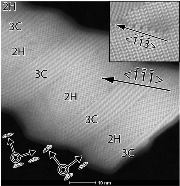
Several 3C (cubic) and 2H (hexagonal) domains along the bottom of a Si(111) nanowire.
The final steps will be to characterize this new material with collaborators on its electrical and optical properties. Since the process is CMOS compatible, an attempt will be made to try to make the first steps towards a hexagonal phase Si-Ge laser, and/or the production of wafer scale hexagonal Si-Ge.
CV
Internship UNSW Sydney
Designing, Assembling and Testing a 4 Kelvin Fast Amplier for Quantum Experiments (University of New South Wales, CQC2T)
Master project
Germanium In-Plane Selective Area Growth Nanonetworks on Silicon (Eindhoven University of Technology, AND)

Email address
theo.van-den-berg@c2n.upsaclay.fr
Office number
C101
Address
C2N
10 Bd Thomas Gobert
91120 Palaiseau FRANCE
Phone number
+33 1 70 27 04 88
Research areas
