Allotropism in group-IV semiconductors
Contact: Laetitia Vincent
Silicon and Germanium crystallize in the cubic diamond structure 3C with which they dominate definitely the electronics. Playing on crystal polytypism in semiconductors occurs to be a valuable mean of electronic band engineering and conduction tuning subsequently creating new functionalities.
Remarkably, changing the crystal structure of SiGe into the hexagonal 2H phase turns to make it a direct band gap with potential emission light. This would finally unlock the gateway of the photonics integration on silicon.
Si and Ge bulk do not display allotropism in standard P-T conditions. The synthesis (pressure, indentation, epitaxy…) of allotrope single crystals or heterostructures in a controlled manner represents a great challenge. The growth of nanowires has initiated a new impetus to this effort. Besides, new paradigms such as selective area growth or remote epitaxy open plenty of rooms to explore for novel phase synthesis.
We explore different ways to synthesize the very promising hexagonal 2H phase of Si and Ge and we examine their properties in order to propose novel "more-than-Moore" applications of SiGe-2H and 2H/3C heterostructures.
Phase transformation in Si nanowires
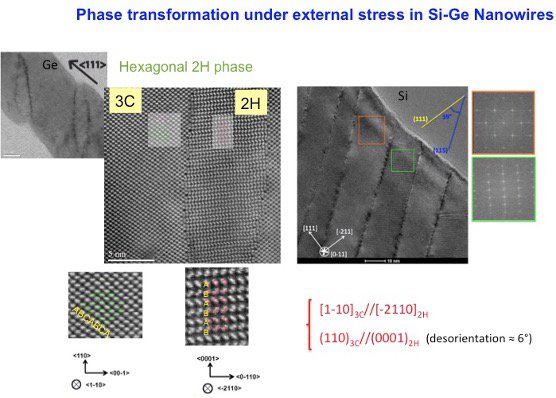
We have pioneered an original method to achieve a shear-induced phase transformation in Ge and Si nanowires resulting in unprecedented heterostructures with quasi periodic embedded 2H domains with abrupt interfaces all along the <111>-oriented nanowire.
Our studies aim at understanding the mechanisms of this martensitic phase transformation and especially the involved size effects. The transformed 2H domains may potentially become seeds for further epitaxial regrowth and integration at larger scale.

Figure: Phase transformation under external stress in Si-Ge Nanowires
These novel axial allotrope heterostructures in Si nanowires provide substantial benefits for phonon dispersion promising thermoelectrics applications for which the use of standard Si technology processes in our concept strongly reinforces the applicability at a device level.
In a framework of a collaboration with SOLEIL Ailes Beamline we also study the decompression pathways in bulk and nanowires using diamond anvil cells.
Epitaxial Synthesis of Ge-2H
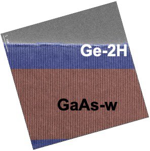
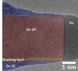
Another way to obtain Ge-2H is to transfer a lattice matched hexagonal structure by epitaxy. GaAs-wurtzite nanowires are ideal templates for Ge-2H epitaxy. Ge-2H grows with a perfect hexagonal structure on GaAs-(1-100) surfaces. By real-time TEM observations we study the growth modes of Ge-2H with UHV-CVD and the formation of stacking defects in core-shell structures.


Works include the exploration of adequate bulk substrates and innovative growth modes such as nanowire VLS growth, selective area growth and remote epitaxy for the synthesis of SiGe-2H with tunable Si content.
The planar SiGe-2H integration on silicon would finally provide the long missing brick for the realization of light emission laser on chips.
Growth of SiGe-2H nanowires
We aim at growing SiGe2H nanowires with controlled concentration and controlled doping for electronics and photonics applications

Recent publications
Hexagonal Silicon-Germanium Nanowire Branches with Tunable Composition A. Li, H.I.T. Hauge, M.A. Verheijen, and E.P.A.M. Bakkers, R.T. Tucker, L. Vincent, C. Renard, Nanotechnology 34-1 (2022) 015601. https://iopscience.iop.org/article/10.1088/1361-6528/ac9317
Growth-Related Formation Mechanism of I3-Type Basal Stacking Fault in Epitaxially Grown Hexagonal Ge-2H
L. Vincent, E. M. T. Fadaly, C. Renard, W. H. J. Peeters, M. Vettori, F. Panciera, D. Bouchier, E. P. A. M Bakkers, M. A. Verheijen, Advanced Materials Interfaces 9 -16 (2022) 2102340
https://onlinelibrary.wiley.com/doi/full/10.1002/admi.202102340


