
Heterogeneous integration on silicon
Contact: Charles Renard
Several technical solutions for GaAs monolithic heteroepitaxy on silicon have been studied for more than 30 years. But until now, no large scale and effective process was found to efficiently reduce the dislocation density down to 104-105cm-2 required for CMOS technology. Significant improvements have been reported for many years, thanks to selective area epitaxy of GaAs on Si substrates patterned with dielectric films. However, these layers are inappropriate for applications involving electronic transport between GaAs and Si at a large scale.
To overcome these problems, we have developed a technique based on the Epitaxial Lateral overgrowth on Tunnel Oxide from nano-seed of micrometer scale GaAs crystals on an ultra-thin silicon oxide from nanoscale Si seeds. This method permits the integration of high quality and defect-free crystalline GaAs on Si substrate and provides active GaAs/Si heterojunctions with efficient carrier transport through the thin SiO2 layer. The nucleation from small width openings avoids the emission of misfit dislocations and the formation of antiphase domains. This epitaxial technique paves the way to hybrid III–V/Si devices that are free from lattice-matching restrictions, and where silicon not only behaves as a substrate but also as an active medium.
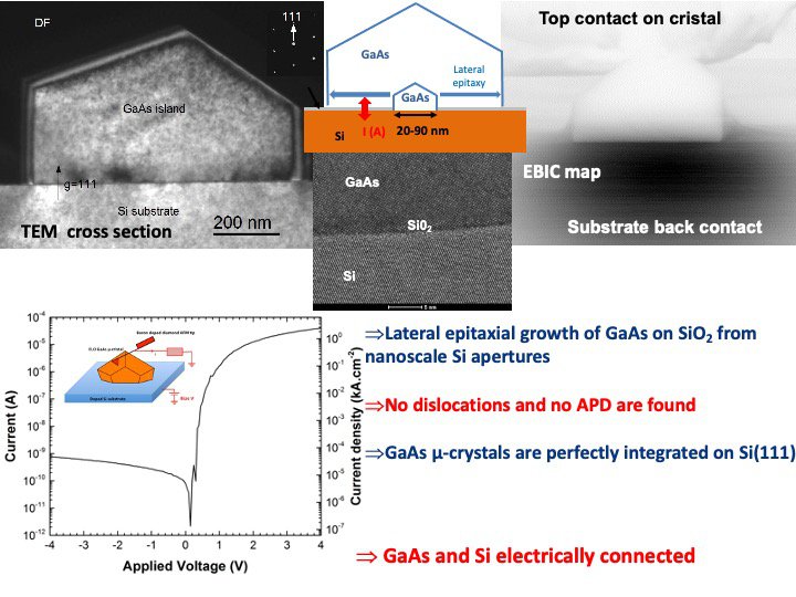
Figure: GaAs heterogeneous integration obtained by epitaxial lateral overgrowth on tunnel oxide from nano-seed
This epitaxial technique paves the way to hybrid III–V/Si devices that are free from lattice-matching restrictions, and where silicon not only behaves as a substrate but also as an active medium.
